For the past 40 years, Si has been the main material choice for manufacturing integrated circuit (IC). Owing to Moore’s Law, it achieves unprecedented system integration that shapes our modern life. However, fundamental physical limits of Si present major stumbling blocks for continuous advancement of Si-based ICs. In the “post Moore Era”, to enable further miniaturization (“More Moore”) and functionalization (“More than Moore”) to meet the requirement of lower power consumption as well as high operation speed for smart gadgets driven by societal needs, introduction of novel materials and new device structure is a prerequisite. Our group is always devoted to develop breakthrough microelectronic devices that integrate emerging concepts both on material and device structure innovation to impact next-generation green electronics for sustainable future.
“Green electronics” represents not only a novel scientific term but also an emerging area of research aimed at developing electronic devices that can be operated at lower voltage with high performance. Our group is interested in developing the following devices with the aim to achieve green electronics. If you are desperately striving for excellence and pleased to face work that is challenging and creative, come join us!
過去40年,矽一直是製作積體電路的主要材料。歸因於摩爾定律 (Moore’s Law),歷經了數十年的演進,積體電路已達到了前所未有的系統整合並形塑了今日智慧生活的樣貌。然而,以矽為主的積體電路製程也因為物理極限之故而面臨了極大的挑戰。在後摩爾時代(post Moore Era),如何實現進一步的微縮化(More Moore)與功能多樣化(More than Moore)以滿足智慧裝置低功率/高效能之需求,導入新穎的材料與創新的元件結構是一項不可避免的趨勢。本團隊致力於整合開創性的材料與結構,目標是實現滿足永續環境的綠能電子元件。所謂的綠能電子元件不僅是一個科學名詞,更代表了一個新興的研究領域,期盼以更低的能耗成就更高功效的電子元件。本團隊目前正在開發的綠能元件整理如下,其中關於鐵電記憶體的內容可以參考以下的連結。若你具有追求卓越的DNA並樂於面對有創意的研究,歡迎加入我們!
1. Ferroelectric memory in the form of FeFET and FTJ with high operating speed and robust reliability by structure and material engineering
以結構與材料工程實現高效能與高可靠度之FeFET與FTJ鐵電記憶體
2. Neuromorphic computing beyond Von Neumann architecture by using ferroelectric material based neuron and synapse
以鐵電材料之神經元與突觸元件實現神經型態運算超越馮·諾伊曼運算架構
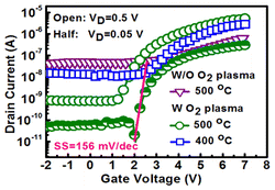
3. Transistors with augmented drive current by integrating with high-mobility channel such as Ge and GeSn
以高載子遷移率之Ge或GeSn作為電晶體通道材質提升電性效能
4. Contact and metal gate process development for advanced VLSI technology
開發適用於先進元件之接觸金屬與閘極製程